Daniel sent us this one — he's asking what somebody does when they want a custom piece of hardware, something like a pocket beacon light, and nobody sells one. You've got the coding skills, you've got the ESP32 or Arduino, you've breadboarded the thing, but now you're staring at a blank PCB editor and you have no idea where to start. What software do you use? What's the most basic level you can begin from? And is simulating your circuit on the computer before you order boards actually a thing hobbyists do, or is that just industry stuff bleeding into YouTube tutorials?

This is the exact wall I see people hit. They can write firmware, they can wire a breadboard, but the moment the screen shows a black canvas with a grid they freeze. And the wild thing is — it's never been easier to cross that gap. The tools are free, the libraries are enormous, and you can get five copies of your board delivered for less than a sandwich.
Less than a sandwich in this economy is saying something.
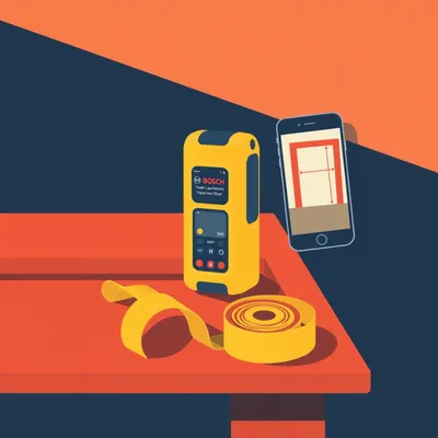
I'm serious. JLCPCB charges about two dollars for five copies of a two-layer board, a hundred by a hundred millimeters. Shipping to most countries is around five bucks. So you're in for seven dollars total, and that's your entire financial risk on a first board.
The barrier is psychological, not financial.
That's the whole episode right there. The barrier is psychological, not financial, and not even really technical. Let's define who we're talking about here. This is someone who can write code, who's comfortable with an ESP32 or an Arduino, who's probably built something on a breadboard or perfboard, but has never laid out a copper trace. They've never opened a PCB editor. And they're wondering — do I need to learn circuit theory? Do I need to understand Ohm's law at a deep level? Do I need to model every component from scratch?
The answer to all of those is no, which is going to sound like heresy to some people.
It's not heresy, it's just honest about what ninety percent of hobbyist projects actually require. Let's break down what designing a PCB actually means. There are three layers. First is schematic capture — that's the logical diagram. You're drawing which pins connect to which, you're placing symbols for resistors and capacitors and your microcontroller. Second is component footprint assignment — that's where you take those abstract symbols and say, this resistor is an 0805 surface-mount package, this ESP32 module is the WROOM thirty-two with castellated edges. Third is board layout — actually placing those physical footprints on a board outline and drawing the copper traces between them.
We're going deep on the first two today, and enough of the third to get a working board, not a production-optimized one.
This is not about designing something you'd sell on DigiKey. This is about getting a functional board into your hands.
The first thing somebody sees when they open PCB software is an empty project. What does that actually look like? Is it a blank text editor equivalent, or is it already asking you for things you don't understand?
Let me walk through the three tiers of tools, starting with the one that requires literally zero installation. It's browser-based, it's free, and as of now in twenty twenty-six it has over five hundred thousand component footprints in its library. You go to the website, you click create project, and you get a blank schematic sheet. That's it. No configuration wizard, no project settings you need to understand. Just a white canvas with a grid.
Five hundred thousand footprints. So the odds that you need to draw a component yourself are basically zero for an ESP32 project.
Essentially zero for anything involving standard modules. The ESP32-WROOM-thirty-two has standardized two-point-five-four millimeter pitch castellated edges. Every library in every tool has it. You search ESP32-WROOM, you drag it onto your schematic, and it already knows what the physical footprint looks like. You don't think about the footprint until you switch to the PCB editor, and even then it's just...
What does the actual workflow look like in EasyEDA? Somebody sits down, they want to build a minimal ESP32 circuit. What are they clicking?
Step one, create a new project. Step two, you're in the schematic editor. On the left sidebar there's a library panel. You type ESP32-WROOM-thirty-two into the search bar. It pops up. You click it, you click place on the canvas. Now you've got the symbol — a rectangle with all the pin labels. Step three, you need power. You search for a three-point-three-volt regulator — the AMS1117-three-point-three is in the library. You need decoupling capacitors — search for a zero-point-one microfarad ceramic capacitor, place two of them near the regulator. You need an EN pin pull-up resistor — a ten-kilohm resistor, search, place. You need a USB-to-UART bridge — the CP2102 or CH340C, both in the library. You need one GPIO output to an LED with a current-limiting resistor — place an LED, place a two-hundred-twenty-ohm resistor.
At this point you're just connecting pins with virtual wires.
You're drawing nets. You click the wire tool, you click pin one, you click pin two, and it draws a line. That line represents a copper connection on the final board. You wire VCC from the regulator to the ESP32's VCC pin. You wire ground to ground. You wire the EN pin through that ten-kilohm resistor to three-point-three volts. You wire the CP2102's TX and RX to the ESP32's RX and TX, crossed. You wire the LED through the resistor to GPIO twenty-one.
This sounds suspiciously like the breadboard wiring they already know how to do, just drawn instead of physical.
That's exactly what it is. And that's the insight that makes the psychological barrier collapse. If you can wire a breadboard, you can draw a schematic. The schematic is just a breadboard diagram with cleaner lines.
Then what happens? You've drawn all your connections. You click something and magic happens?
You click a button that says convert to PCB. EasyEDA asks you to confirm the board outline — it defaults to a rectangle, you can adjust the dimensions. Then it switches you to the PCB editor. All your components appear as footprints — little white outlines with silver pads — arranged off to the side of the board. You drag them onto the board. You arrange them roughly where you want them. And then you start routing — you click the track tool, you click one pad, and you draw a line to the other pad. The software shows you thin blue and red lines called ratsnest — those are the connections you defined in the schematic, telling you what needs to connect to what. You just follow the lines.
At some point you hit a button that checks whether you've made any obvious mistakes.
Design rule check. You set your minimum trace width — I'd say zero-point-three millimeters for a beginner — and your minimum clearance between traces, also zero-point-three millimeters. You run the check, and it tells you if any traces are too close together or if you forgot to connect something.
That's Tier One. Browser-based, free, integrated library, integrated manufacturing. What's the catch?
The catch is it's cloud-dependent. Your projects live on EasyEDA's servers. If their service goes down, you can't access your work. And it's owned by LCSC, which is the same company that runs JLCPCB. So you're in an ecosystem. Which is honestly fine for a first board — the integration means you can click export Gerber files and upload directly to JLCPCB in two clicks. But some people want something that lives on their own machine, with no account required. That's KiCad.
The Tier Two option.
KiCad is the open-source heavyweight. Version eight-point-zero released in February twenty twenty-four, and it's a serious piece of software. It added a built-in trace width calculator and improved push-and-shove routing — that's where you drag a trace and it automatically pushes other traces out of the way. But the key difference from EasyEDA is that KiCad separates the schematic editor and the PCB editor as distinct applications. You open KiCad, you get a project manager window. You click schematic editor, it opens one application. You finish your schematic, you click PCB editor, it opens a different application.
Which sounds like it would be disorienting for someone who's never done this.
It is, at first. But it also enforces a mental model. Schematic is logical, PCB is physical. They're separate concerns. And KiCad's component library system is different — you don't search a single unified library. You browse footprint libraries by category. There's a learning curve, but the payoff is that you own everything. No account, no cloud, no internet connection required. Your files are local. And the community library ecosystem is enormous — the ESP32-WROOM footprint is available through KiCad's package manager.
Then there's Tier Three, which is Fritzing. I have opinions about Fritzing.
I know you do.
Fritzing is the tool that lets you draw a breadboard view — literally drag and drop components onto a virtual breadboard — and then it auto-converts to a schematic and a PCB. It's designed for visual learners. And it produces layouts that look like a toddler arranged the components by throwing them at the board.
not entirely unfair. Fritzing's auto-router makes aesthetic choices that no human would make. Traces take wildly inefficient paths. Components end up in baffling locations. It works for something with ten components or fewer — a simple LED blinker, a basic sensor readout. Beyond that, you're fighting the tool.
The musical equivalent of beige wallpaper. It technically covers the wall, but you wouldn't invite anyone to look at it.
Here's the thing — Fritzing hasn't been actively developed in years. The component library is stagnant. If you're going to invest time learning a tool, learn one that scales with you. EasyEDA for the first board, KiCad for everything after.
We've got the tools. But there's this other question lurking in the prompt — what's the blank slate? When someone opens EasyEDA or KiCad, are they expected to model components themselves? Are they drawing little resistor bodies from scratch?
And this is the misconception that scares people away. They think PCB design means creating every component from a blank canvas — defining the pin layout, the physical dimensions, the silkscreen outline. For ESP32 and Arduino projects, you almost never do this. The libraries have everything. ESP32 modules, Arduino Nano footprints, every common sensor breakout, every standard passive component. You only create custom footprints when you're using something genuinely obscure — a weird mechanical switch, a custom connector, a sensor from a niche manufacturer that hasn't been library-fied yet.
Even then, you're usually just copying dimensions from a datasheet into a footprint editor. You're not inventing anything.
You're transcribing. The datasheet gives you the pad dimensions, the pitch, the courtyard. You type those numbers into a dialog box. It's data entry, not design.
The blank slate is blank — but the things you put on it are pre-built. You're assembling, not sculpting.
Think of it like software development. When you start a new project, you don't write your own HTTP library. You import one. Same thing here — you're importing component models from libraries. The blank schematic sheet is your empty main-dot-c file, and the component library is your package manager.
Let's make this concrete. Somebody wants to build that pocket beacon light we talked about. What does the actual circuit look like, and how do they lay it out?
The pocket beacon needs an ESP32 for control and Bluetooth, a LiPo battery charger — that's a TP4056 module — a boost converter to drive a high-power LED, so an MT3608, and a MOSFET to switch the LED on and off. Let's walk through the schematic. You place the ESP32-WROOM symbol. You place the TP4056 — it has a standard charging circuit with a few passives, all in the library. You place the MT3608 boost converter — again, standard application circuit from the datasheet, the components are all in the library. You place a logic-level N-channel MOSFET — something like an AO3400 — and you connect its gate to an ESP32 GPIO pin through a small resistor.
The power budget?
Here's where the calculation comes in, and this is important. The ESP32 in active WiFi mode draws about eighty milliamps. The high-power LED might draw a hundred and fifty milliamps. The boost converter is maybe eighty-five percent efficient. So total draw from the battery is roughly two hundred seventy milliamps. You look at the IPC-twenty-two-twenty-one standard for trace width — one ounce copper, ten degrees Celsius temperature rise. A one-millimeter-wide trace handles about one-point-five amps. Your two hundred seventy milliamps needs a trace width of roughly zero-point-three millimeters on one-ounce copper. That's tiny. You have massive safety margin.
You're not doing complex thermal simulation. You're looking at a chart and doing arithmetic.
You're looking at a chart. Or better yet, you're using KiCad's built-in trace width calculator. You type in your current — two hundred seventy milliamps — your copper weight — one ounce — your allowed temperature rise — ten degrees — and it spits out zero-point-two-six millimeters. You round up to zero-point-three and move on.
Which brings us to the elephant in the room. The thing that professional EEs do with LTSpice and Ansys and HyperLynx. Is any of that relevant here?
For an ESP32 hobbyist project, simulation provides zero benefit over rule-of-thumb design. And I want to be precise about why. SPICE simulation — that's Simulation Program with Integrated Circuit Emphasis — models analog circuits at the transistor level. You define a circuit, you define voltage sources, and the simulator solves differential equations to tell you voltages and currents at every node. It's essential for analog design — op-amp circuits, filters, power supply stability. But here's the problem: the ESP32 itself is a black box. There is no public SPICE model for the ESP32. There is no SPICE model for the CP2102 USB bridge. There is no SPICE model for most of the ICs you're using. You can't simulate what you can't model.
The thing people see in professional workflows — engineers running simulations before they tape out a chip — that's for a completely different class of problem.
That's for eight-layer boards with DDR4 memory running at three thousand two hundred mega-transfers per second. That's for RF antenna matching where a millimeter of trace length changes the impedance. That's for power integrity on a board that draws fifty amps. None of that applies to a two-layer ESP32 board running at forty megahertz SPI. The signal integrity rules you need for USB — keep the data lines under fifty millimeters, match their lengths within five millimeters, avoid ninety-degree corners — those come straight from the USB two-point-zero specification. You don't simulate them. You follow the spec.
What does the hobbyist actually do instead of simulation?
First, you calculate your power budget from datasheet numbers — peak current draw, average current draw, battery capacity. Second, you size your traces using the IPC standard charts or the calculator built into your tool. Third, you verify with a multimeter after assembly. That's it. Measure the actual current draw. Check for voltage droop. Feel if anything's getting hot. The ESP32 can hit eighty-five degrees Celsius under heavy load — that's within spec, but you want to keep heat-sensitive components like battery chargers at least five millimeters away from the module.
The datasheet is your simulation.
The datasheet is your simulation. And for sub-ten-megahertz digital circuits — which covers all ESP32 GPIO, I2C at four hundred kilohertz, SPI at forty megahertz — manual calculation and datasheet adherence produce identical results to simulation. The only time simulation matters for hobbyist work is if you're doing something with RF — antenna matching, impedance-controlled traces for a custom PCB antenna. And honestly, if you're doing that on your first board, you've already made a mistake.
Let's say I've accepted all of this. I've downloaded EasyEDA. I've drawn my schematic. I've routed my board. How do I actually get physical boards in my hands?
You export Gerber files. Gerber is the standard format for PCB manufacturing — it's a set of files, one for each layer. Copper top, copper bottom, soldermask top, soldermask bottom, silkscreen top, drill file, board outline. EasyEDA has a one-click export. KiCad has File, Plot, Generate. You zip those files. You go to JLCPCB dot com or PCBWay dot com. You upload the zip. Their system renders a preview of your board. You select options — two layers, one-ounce copper, green soldermask, lead-free HASL finish, one-point-six millimeter board thickness. You click order.
Seven dollars later, you're waiting for a package from Shenzhen.
About a week for the cheapest shipping. And when the boards arrive, they look professional. Green soldermask, white silkscreen, gold pads. It feels like you've done something real.
Which you have. You've manufactured a thing.
Here's the part I want to emphasize — your first board will have mistakes. Something will be wired backwards. A footprint will be wrong. You'll forget a pull-up resistor. This is normal. This is expected. Plan for two or three revision cycles. Each revision costs you about five dollars for five boards. That's your learning tuition. Fifteen dollars total to go from never having touched a PCB editor to holding a working custom board.
That's less than a textbook.
It's less than a nice lunch.
Let's flip this around. We've talked about what you don't need to do. No simulation, no component modeling, no circuit theory deep dives. What's the actual minimum viable workflow? Somebody's listening to this, they want to start tonight. What do they do?
Step one, download EasyEDA or open it in your browser. No install, no account setup beyond an email address. Step two, find a reference design for your microcontroller. Espressif publishes the ESP32-DevKitC schematic publicly — it's the official development board schematic. Copy the power section verbatim. The three-point-three-volt regulator, the decoupling capacitors, the EN pin pull-up, the USB-to-UART bridge. Don't innovate on the power section. Copy what works.
Copying the power section of a reference design is the hardware equivalent of using a boilerplate web framework. You don't write your own authentication system on your first web app. You don't design your own power regulation on your first PCB.
Step three, add your custom components. Your LED driver, your sensor, your MOSFET switch. These are the parts that make your board unique. They're the reason you're designing a PCB instead of buying a dev board. Step four, route your traces. Minimum trace width zero-point-three millimeters, minimum clearance zero-point-three millimeters. Use the autorouter if you want — it'll get you eighty percent of the way there — then clean up the weird paths manually. Step five, run design rule check. Step six, export Gerbers and upload to JLCPCB.
That's an evening's work.
If you know what components you need and you have a reference schematic open, you can go from blank screen to uploaded Gerbers in three or four hours. The first time will take longer because you're learning the tool. The second time will be half that.
You mentioned KiCad is for your second project. What's the inflection point where someone should switch?
When you start hitting EasyEDA's limitations. When you want version control for your designs — KiCad files are plain text, you can put them in Git. When you want to do four-layer boards — EasyEDA can do them, but KiCad's layer stack manager is better. When you want to use community plugins for things like differential pair routing or length tuning. When you want to own your toolchain end to end without a cloud dependency. But none of those matter for a first board. For a first board, you want the path of least resistance, and that's EasyEDA.
What about Arduino-specific boards? If someone's building around an Arduino Nano instead of a raw ESP32 module?
Same workflow, even simpler. The Arduino Nano is a through-hole board with standardized pin headers. You place a Nano footprint — it's in every library — you connect your peripherals to the header pins, and you're done. You don't need to worry about the Nano's power regulation or USB interface because it's all on the module. You're basically designing a custom shield, just in a single-board form factor.
Which is a good way to think about it. A custom PCB is just a breadboard where the wires are copper traces and the components are soldered instead of pushed into spring contacts.
That's exactly the mental model. If you've built something on a breadboard and it works, you already know the circuit. The PCB is just a permanent version of that breadboard.
There's one thing we haven't addressed, which is the component sourcing side. You design a board with an ESP32-WROOM module, you order the boards, and then you need to actually buy the components and solder them on.
This is where EasyEDA's integration with LCSC shines. Every component you place from the library has an LCSC part number attached. You can export a bill of materials — a BOM — and upload it directly to LCSC's website. It populates your shopping cart with all the parts. The ESP32-WROOM-thirty-two module costs about three to four dollars in single quantities. Passives are fractions of a cent. A full BOM for a pocket beacon light — ESP32, charger IC, boost converter, MOSFET, LED, resistors, capacitors, connectors — probably lands around twelve to fifteen dollars.
Plus the seven dollars for the boards, you're at about twenty dollars for a custom device that doesn't exist on the market.
You have five of them. Keep one, give one to a friend, put one in a drawer, break one while soldering, and have a spare.
The economics of custom PCBs are absurd.
They're absurd because the Chinese PCB industry has optimized for prototyping at a scale that shouldn't be economically viable. They aggregate hundreds of small orders onto a single panel, so you're sharing panel space with other people's designs. Your five boards are cut from a panel that has fifty other designs on it. That's how they hit the two-dollar price point.
What you're saying is we're all subsidizing each other's weird hobby boards.
We're all sharing a panel in Shenzhen. It's beautiful.
Let me ask you about one more thing that comes up in forums. People post their first PCB layouts for review, and the comments are brutal. Trace length matching, ground planes, via stitching, impedance control. Half of it sounds like a different language. How much of that actually matters for a first board?
Almost none of it. Ground planes — yes, you want a solid ground pour on the bottom layer. EasyEDA and KiCad both do this with two clicks. It reduces noise and makes routing easier because every ground connection just goes to the plane. Via stitching — that's placing lots of small vias connecting ground planes on different layers. For a two-layer board running at ESP32 speeds, the ground plane is on the bottom and components are on top, so you don't need via stitching. Impedance control — that's for USB and antenna traces. For USB, just keep the data lines short and matched. For the antenna on the ESP32 module, it's built into the module — you don't touch it.
The forum people are optimizing for problems you don't have.
They're applying professional RF and high-speed digital rules to hobbyist boards that don't need them. A two-layer board with an ESP32 module is forgiving. The module itself handles the hard stuff — the antenna matching, the crystal oscillator, the RF shielding. You're just providing power and connecting GPIO pins.
The module is doing all the heavy lifting, and you're building it a little house.
You're building the ESP32 a house with good plumbing and some nice light fixtures.
That house has a front door, which is the USB connector, and windows, which are the pin headers. I've extended this metaphor too far.
You have, but I appreciate the commitment.
Let's talk about the thing that actually kills first boards. Not design mistakes — those are fixable. What's the thing that makes someone give up?
They read forum posts about impedance-controlled differential pairs and think they need to understand all of it before they start. They watch a professional PCB design tutorial where someone is routing DDR4 memory on a twelve-layer board and they think that's what PCB design is. It's not. PCB design for a hobbyist ESP32 project is connecting dots. The software tells you which dots need connecting. You draw the lines.
The software also tells you when you've made a mistake.
The design rule check catches the obvious stuff. Shorts between nets, traces too close together, unconnected pins. It won't catch logic errors — if you wire the LED to the wrong GPIO pin, the DRC won't flag that. But that's the same class of bug as a software logic error. You test it, you find it, you fix it in the next revision.
We've covered tools, workflow, what to skip. What about the mechanical side? You've got a bare PCB, it works, but it's just a green board with components. How do you turn it into something you'd actually carry in your pocket?
That's the next frontier, and honestly it's where I see more people get stuck than with the PCB itself. Enclosures, battery connectors, power switches — the mechanical design that turns a PCB into a device. You can 3D print an enclosure, you can use off-the-shelf project boxes, you can design something in Fusion three-sixty and have it CNC milled. But that's a whole separate skill set.
We should probably do a whole episode on that. The jump from working board to finished product.
And there's an emerging angle here too — AI-assisted PCB design. Companies like CircuitMind and Altium are building AI routers that can place components and route traces automatically. As of twenty twenty-six, these are still slower than a human for simple boards — the AI overhead isn't worth it for a two-layer ESP32 design. But that's going to change within two or three years. The same way GitHub Copilot changed software development, AI routers are going to change PCB design. For now, manual routing is faster for simple boards. But the writing is on the wall.
The window for learning manual PCB design as a distinct skill might be closing.
Learning manual routing will always have value for understanding what's happening under the hood. But for the hobbyist who just wants a working board, AI routers are going to make the "blank screen" problem disappear. You'll describe your circuit in natural language, and the AI will generate a schematic and a layout. We're not there yet, but we're closer than most people realize.
Which makes now a surprisingly good time to learn the fundamentals. You'll understand what the AI is doing, and you'll know when it's doing something stupid.
Which it will. AI routers do baffling things sometimes. Knowing enough to catch those mistakes is going to be a valuable skill.
Alright, let's bring this home. Someone listening wants to start tonight. Give them the single-sentence recommendation.
Go to EasyEDA dot com, create an account, open a new project, search for ESP32-WROOM-thirty-two in the library, place it on the schematic, and start connecting things.
If they get stuck?
Espressif's hardware design guide is public and free. The ESP32-DevKitC schematic is public and free. There are hundreds of open-source ESP32 PCB designs on GitHub that you can study. Copy what works. Don't innovate on power regulation. Don't simulate anything. Don't worry about impedance. Just connect the dots and order the boards.
The first board is about learning, not perfection.
The first board is about proving to yourself that you can do it. Everything after that is refinement.
If someone listening does build that pocket beacon light — or any first PCB — we want to see it.
Send us photos. Send us the lessons you learned. Send us the mistakes you made so other people can avoid them. We'll feature community builds in a future episode. If you build it, we want to see it.
We should also mention — if you're enjoying the show and you haven't left a review, it helps. Wherever you listen, drop us a rating. It makes a difference.
Now: Hilbert's daily fun fact.
Hilbert: A nineteen fifty-three agricultural extension pamphlet from Funafuti, Tuvalu, recommends curing a traditional earth oven by glazing the interior with fermented coconut cream and crushed coral sand, then firing it with pandanus husks for six hours. The pamphlet notes this produces a "vitreous, non-porous lining superior to imported cast iron.
...vitreous lining. From coconut cream and coral.
Superior to imported cast iron.
This has been My Weird Prompts. Thanks to our producer Hilbert Flumingtop. I'm Corn.
I'm Herman Poppleberry. We'll be back next week.

")